Many AVR microcontrollers are capable of doing Analogue to Digital Conversion. The ATmega168 has 6 ports (8 ports on the SMD packages) that can be used for analogue input. This tutorial shows you how.
The circuit
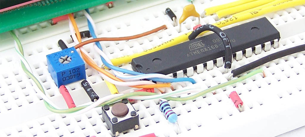
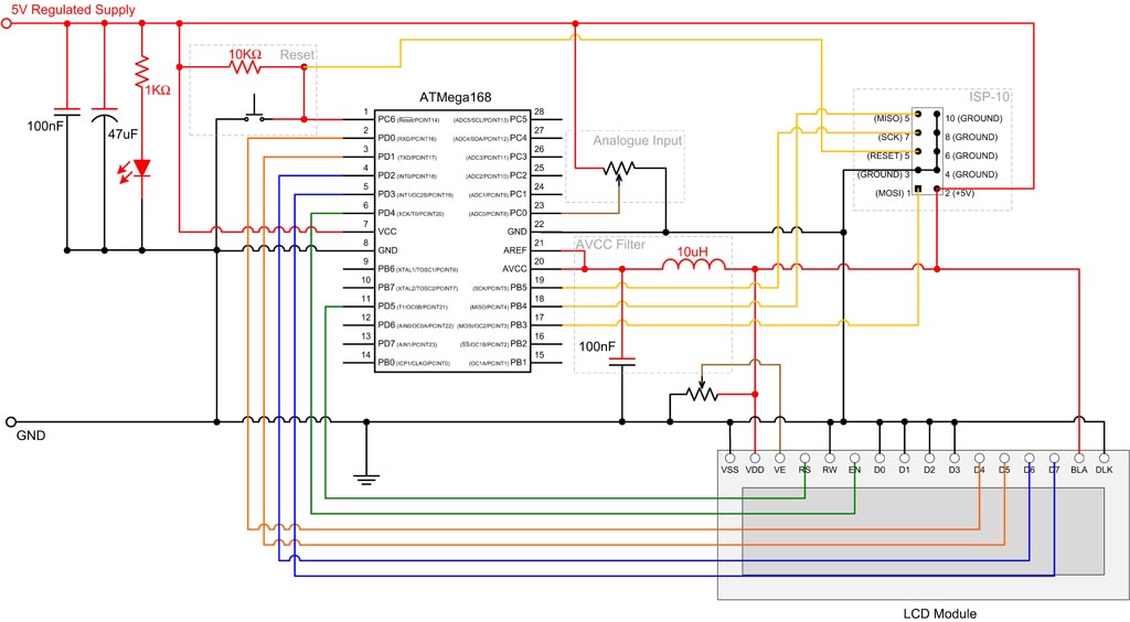
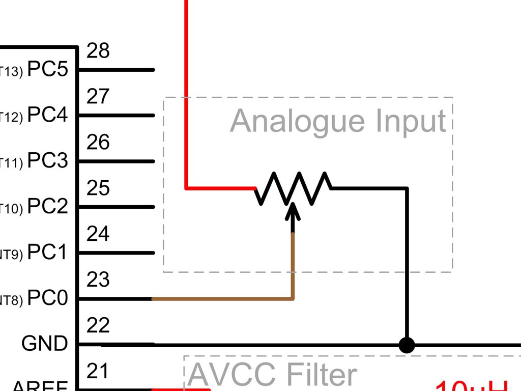
We’ll be building the following circuit on a breadboard.
The Breadboard layout is based on the Atmega8 breadboard circuit which is described in Atmega8 breadboard circuit Part 1 and Atmega8 breadboard circuit Part 2.
AVCC
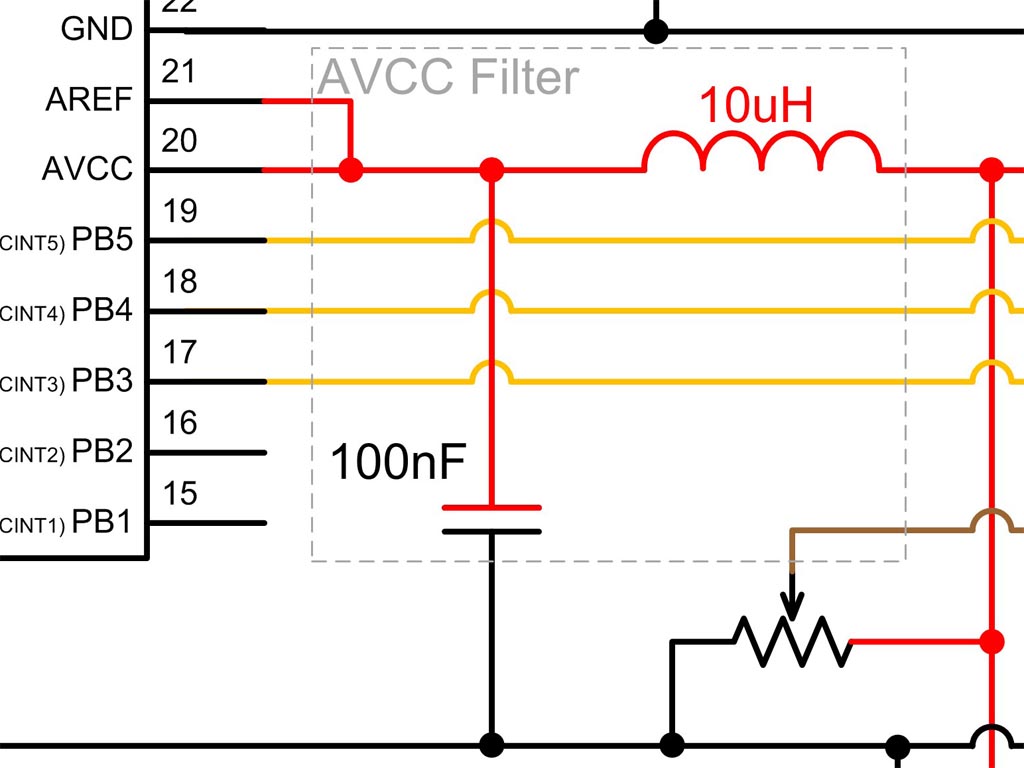
The Atmega168 has 2 digital supply voltage pins, VCC and AVCC. AVCC supplies power to PC0-PC5. When these pins are used as analogue inputs, the AVCC power needs to be very stable. This is achieved by using a low pass filter comprising of an inductor and capacitor.
AREF
The AREF pin is used to set the voltage that corresponds to a 100% value (1024) in the AD converter. In this example we tie it to AVCC.
Analogue Input
The Atmega168 has has 6 pins (8 for the SMD packages) that can be used for analogue input. These are PC0 to PC5. These are normally used for digital I/O but can be used for analogue input as well. In our example we are using a trimpot as the analog input device and connecting it to PC0.
LCD display
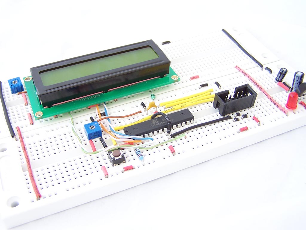
We’ve connected an LCD display to pins PD0 to PD5 and is used to display analogue readings. For more information on using LCD displays, please read Character LCD Displays – Part 2.
Registers
The Atmega168 uses 6 different registers when performing analogue to digital conversion. These are:
| Register | Description |
|---|---|
| ADMUX | ADC Multiplexer Selection Register |
| ADCSRA | ADC Control and Status Register A |
| ADCSRB | ADC Control and Status Register B |
| DIDR0 | Digital Input Disable Register 0 |
| ADCL | ADC Data Register – Low |
| ADCH | ADC Data Register – High |
The ADMUX register allows you to control:
- The Reference Voltage
- Left adjustment of results (used for 8 bit results)
- Selection of input channel
| bit | 7 | 6 | 5 | 4 | 3 | 2 | 1 | 0 |
|---|---|---|---|---|---|---|---|---|
| ADMUX | REFS1 | REFS0 | ADLAR | – | MUX3 | MUX2 | MUX1 | MUX0 |
| Read/Write | R/W | R/W | R/W | R | R/W | R/W | R/W | R/W |
| Initial Value | 0 | 0 | 0 | 0 | 0 | 0 | 0 | 0 |
The reference voltage is controlled by REFS1 and REFS0. The default is to use AREF, but other options are available.
ADLAR is used for left shifting the converted data. This is useful when reading 8 bit values due to the fact that reading a 16 bit value is not an atomic operation.
MUX0 to MUX3 are used to select which input channel you wish to read. The values 0000 to 0101 allow you to select ports PC0 to PC5, while the reserved values of 1110 and 1111 allow you to select 1.1V and 0V.
ADCSRA and ADCSRB are used to control the AD conversion process.
| bit | 7 | 6 | 5 | 4 | 3 | 2 | 1 | 0 |
|---|---|---|---|---|---|---|---|---|
| ADCSRA | ADEN | ADSC | ADATE | ADIF | ADIE | ADPS2 | ADPS1 | ADPS0 |
| Read/Write | R/W | R/W | R/W | R/W | R/W | R/W | R/W | R/W |
| Initial Value | 0 | 0 | 0 | 0 | 0 | 0 | 0 | 0 |
| bit | 7 | 6 | 5 | 4 | 3 | 2 | 1 | 0 |
|---|---|---|---|---|---|---|---|---|
| ADCSRB | – | ACME | – | – | – | ADTS2 | ADTS1 | ADTS0 |
| Read/Write | R | R/W | R | R | R | R/W | R/W | R/W |
| Initial Value | 0 | 0 | 0 | 0 | 0 | 0 | 0 | 0 |
These 2 registers provide for many different options and we will look at a subset in this tutorial.
ADEN enables the AD converter subsystem. This bit needs to be set before any conversion takes place.
ADSC is set when you want to start an AD conversion process. When the conversion is finished, the value reverts back to 0.
ADIF is set when the conversion is complete and the data is written to the result registers (ADCL/ADCH). To clear it back to 0 you need to write a 1 to it.
When an analog sample is read, a timeslice is used. The width of that timeslice is determined by the input clock. ADPS0 to ADPS2 sets the division factor between the system clock and the input clock.
DIDR0 is used to disable the digital input buffers on PC0 to PC5. When set, the corresponding PINC value will be set to 0.
| bit | 7 | 6 | 5 | 4 | 3 | 2 | 1 | 0 |
|---|---|---|---|---|---|---|---|---|
| DIDR0 | – | – | ADC5D | ADC4D | ADC3D | ADC2D | ADC1D | ADC0D |
| Read/Write | R | R | R/W | R/W | R/W | R/W | R/W | R/W |
| Initial Value | 0 | 0 | 0 | 0 | 0 | 0 | 0 | 0 |
Lastly we have the ADC Data Registers, ADCL and ADCH. The AD converter returns a 10 bit value which is stored in these 2 registers. The structure of these registers depends on the ADLAR value.
ADLAR=0
| bit | 7 | 6 | 5 | 4 | 3 | 2 | 1 | 0 |
|---|---|---|---|---|---|---|---|---|
| ADCH | – | – | – | – | – | – | ADC9 | ADC8 |
| Read/Write | R | R | R | R | R | R | R | R |
| Initial Value | 0 | 0 | 0 | 0 | 0 | 0 | 0 | 0 |
| bit | 7 | 6 | 5 | 4 | 3 | 2 | 1 | 0 |
|---|---|---|---|---|---|---|---|---|
| ADCL | ADC7 | ADC6 | ADC5 | ADC4 | ADC3 | ADC2 | ADC1 | ADC0 |
| Read/Write | R | R | R | R | R | R | R | R |
| Initial Value | 0 | 0 | 0 | 0 | 0 | 0 | 0 | 0 |
ADLAR=1
| bit | 7 | 6 | 5 | 4 | 3 | 2 | 1 | 0 |
|---|---|---|---|---|---|---|---|---|
| ADCH | ADC9 | ADC8 | ADC7 | ADC6 | ADC5 | ADC4 | ADC3 | ADC2 |
| Read/Write | R | R | R | R | R | R | R | R |
| Initial Value | 0 | 0 | 0 | 0 | 0 | 0 | 0 | 0 |
| bit | 7 | 6 | 5 | 4 | 3 | 2 | 1 | 0 |
|---|---|---|---|---|---|---|---|---|
| ADCL | ADC1 | ADC0 | – | – | – | – | – | – |
| Read/Write | R | R | R | R | R | R | R | R |
| Initial Value | 0 | 0 | 0 | 0 | 0 | 0 | 0 | 0 |
To make things easier, the AVR libc library returns the values of these registers as a single 16 bit value, ADC.
Putting it all together
The following code example shows how to read an analogue value and output it to the LCD panel.
1 2 3 4 5 6 7 8 9 10 11 12 13 14 15 16 17 18 19 20 21 22 23 24 25 26 27 28 29 30 31 32 33 | #include <avr/io.h> #include "hd44780.h" uint16_t ReadADC(uint8_t __channel) { ADMUX = (ADMUX & 0xf0) | __channel; // Channel selection ADCSRA |= _BV(ADSC); // Start conversion while(!bit_is_set(ADCSRA,ADIF)); // Loop until conversion is complete ADCSRA |= _BV(ADIF); // Clear ADIF by writing a 1 (this sets the value to 0) return(ADC); } void adc_init() { ADCSRA = _BV(ADEN) | _BV(ADPS2) | _BV(ADPS1) | _BV(ADPS0); //Enable ADC and set 128 prescale } int main (void) { lcd_init(); adc_init(); while (1) { char buffer[16]; sprintf(buffer,"%d ", ReadADC(0)); lcd_goto(0); lcd_puts(buffer); } return(0); } |
Sharing is Caring
If you like this post, please post it on twitter, Facebook or your blog. Your support is very much appreciated.

Hi,
Nice write up, just one question. What program did you use to create the schematics?
Microsoft Visio
You don’t need to clear ADIF after conversion. It clears itself (else the while loop would never exit).
Actually, to correct myself, it clears itself when the next conversion is started. Still no need to clear it.
Hello !
I have to disagree with you, but the ADIF flag is NOT cleared when the next conversion is started, it has to be cleared manually. However, the bit ADSC does clear itself after a conversion finishes. Maybe that is what you meant ?
Best regards,
Tom
It clears on the interrupt. That is what is says in the datasheet.
ADIF is set when the conversion is complete. See page 259 of the datasheet (http://www.atmel.com/dyn/resources/prod_documents/doc8025.pdf).
The loop keeps on looping while ADIF is unset. When ADIF is set it terminates.
I’ve had a look through the datasheet, and I can’t find any reference to ADIF being cleared when the next conversion is started, but that doesn’t mean it doesn’t happen.
Check page 265 in the datasheet.
* Bit 4 – ADIF: ADC Interrupt Flag
This bit is set when an ADC conversion completes and the Data Registers are updated. The ADC Conversion Complete Interrupt is executed if the ADIE bit and the I-bit in SREG are set. ADIF is cleared by hardware when executing the corresponding interrupt handling vector. Alternatively, ADIF is cleared by writing a logical one to the flag. Beware that if doing a Read-Modify-Write on ADCSRA, a pending interrupt can be disabled. This also applies if the SBI and CBI instructions are used.
I did not understand the meaning of this line :
“the reserved values of 1110 and 1111 allow you to select 1.1V and 0V”.
Can you please elaborate on this point.
Thanks.
The MUX3-0 values allow you to select a source for the conversion. The 1110 and 1111 values are used for the selection of 1 of 2 reference values. For example selecting 1110 will produce the same result as selecting 0000 while applying 1.1V to ADC0 (PC0).
By the way, the ATMEGA168A has an extra input channel ADC8, to read from the on chip temperature sensor. To select it, simply set MUX3-0 to 1000. When using this channel you need to also set REFS1-0 to 11 which sets the reference voltage to 1.1V.
in what IDE do you write code ?
in this command return(ADC); I don’t understand where you got the variable ADC ?
in the program it is not declared
It is defined in the complier standard C libraries for the AVR controller family. It is not actually a variable, but a macro that stands for a short piece of code that combines the contents of ADCH and ADCL registers into a single 16 bit value – or the equivalent registers of whatever microcontroller you tell it you have. The compiler will replace the macro with that bit of code automatically.
Hello,
Your tutorials are very helpful. Please see if you can help me with the following-
My ADC pins are showing arbitrary values. What could be the possible reason? Also I changed the controller, with Atmega8 (instead of Atmega168), but the problem still prevails.
Can you please help me in measuring AC voltages, using ADC.
Thank You.
The ADC is taking short DC measurements of the AC waveform, so the result you get depends on when you initiate the measurement and what your sampling rate is. It will give the average DC value of the signal at the moment and duration of the measurement, which for a single measurement at a random time will be arbitrary.
To measure AC voltages, one must take multiple measurements at a rate that is at least twice the frequency of the AC waveform you intend to measure, and compute from these samples the required information such as voltage or frequency.
It’s not showing zero, but any arbitrary value, even though the applied voltage is zero.
It seems that the filter you’re proposing has a resonance at 159 kHz and has a very low damping factor, and with realistic component values is seriously underdamped (Q=100), which means any square wave noise in the source voltage will make the filter ring at 159 kHz and actually amplify any noise signal at that frequency by as much as 1.98 times.
Refer to this handy online calculator/analysis tool for further information http://sim.okawa-denshi.jp/en/RLCtool.php
Erkko what you suggest for a better filter. Also input pins require filter else they go mad(i mean literally), any suggestions for designing filter when using pins as input of the microcontroller.
The calculator tool I linked below can be used to design a better filter of the same type. Aiming for a Q value of 1/2 or below produces a filter which will not resonate around any frequency. Just plug in a cut-off frequency as low as possible, and see what kind of components it suggests, and make a resonable compromize for what kind of components you have available.
For example: 1 Ohm, 22 uF, 10 uH will produce a filter with a 10 kHz cutoff frequency and minimal overshoot or ringing. 10 kHz may be too high if you intend to record clean audio, but low enough to filter out most switching noise caused by the CPU itself.
Large capacitance values need to be made out of electrolytic capacitors which don’t have good high frequency response, so adding a small value ceramic or polymer capacitor in parallel is a good idea. Also remember that the filter coil has some amount of resistance as well.
For input debouncing for buttons, a simple RC filter 10-100kOhm and 100nF or so is usually enough. There are plenty of online calculators for that as well, and it’s the same idea. Button debouncing can however be done in software as well, so you don’t necessarily need to add filters – just add a short delay on the first readout and then read the pin again after it’s settled down.